Description:White Noise source using the thermal noise of a 470k resistor. Flat spectrum from 20Hz to 20kHz. Circuit running on two AA batteries. Advantages: predictable noise density and runs on low voltage/low current.
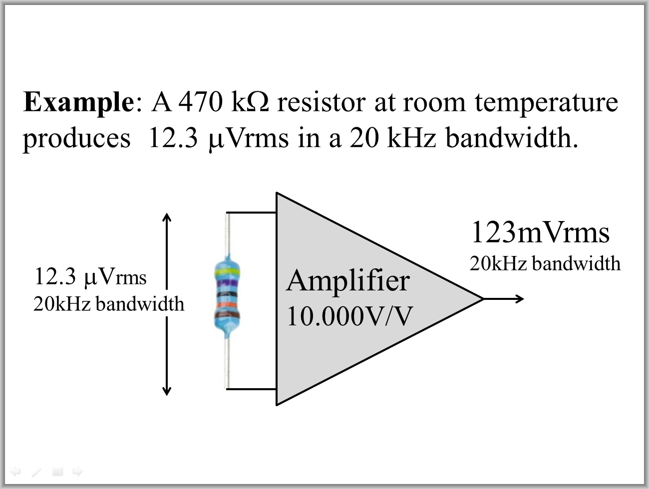
Concept of the noise generator:
The thermal (white) noise voltage of a 470k resistor is amplified up to a level where it can be used as a white noise source for the audio band. If we design the circuit such that resistor noise voltage is dominating then we can accurately predict the output noise density and the noisespectrum will be flat within the amplifier bandwidth.
Circuit diagram, calculations, and measurements on a build prototype are provided. This is quite a simple circuit, but if you have plans on building it, please first read: "points of attention when building this". Amplifying microvolt signals with a gain of 10.000 up to 20kHz makes this a very sensitive circuit, so building quality is key.
The basics for resistor thermal noise:
For a resistor R, the thermal voltage noise = Square root(4KTRB)
Where:
K= a physics constant, Bolzmann's constant=1.38E-23
T= absolute temperature [Kelvin]
R= resistance value [ohm]
B= bandwidth [Hz]
Notes:
One could argue that this noise source amplitude is temperature dependant but for practical use this is a small effect because it relates to absolute temperature (Kelvin). Example: for a temperature change of 20 to 30 celsius the resistor noise voltage changes only by 1.7%, this is 0.6dB. In this circuit we have effectively no current running in the metal film resistor so the thermal noise is the only relevant noise source. For readout a CMOS opamp is used (MCP6021) having small enough input currents to be neglectible (see design considerations).
Circuit output noise density calculations:
Calculations for a 1Hz wide band at 1kHz:
Noise generating resistor value: 470kohm, that gives us 88nV/sqrtHz. Amplified with in total 10201 V/V, this gives us 0.898mV/sqrtHz circuit output noise. Detailled calculations that also include noise of the other resistors and the chosen opamp predict in total 0.915mV/sqrtHz. This is an increase of only 2% so the 470k resistor really sets the noise amplitude.
detailled calculations
Measuring the prototype showed 0.914mV/sqrtHz output noise density and confirms this.
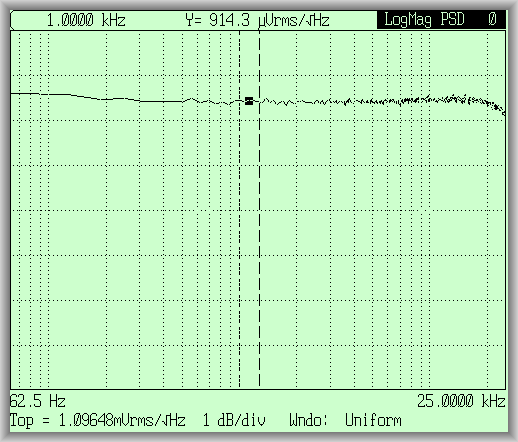
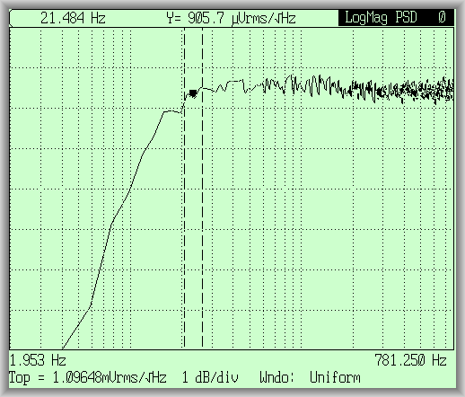
Circuit output noise voltage calculations:
In a 20kHz limited audio band this density results in 129mVrms output noise. On an oscilloscope or other wideband meter you will measure close to 200mVrms. This is caused by the fact that the amplifier response is less than 1dB down at 20kHz and -3dB at 45kHz. That results in a addditional noise "tail" above 20kHz that adds to the wideband oscilloscope reading. Trying to read the peak-peak value is less accurate, this is noise: only statistics are accurate. You will read roughly 1.5Vpp but that is a bit influenced by the timebase setting of your scope.
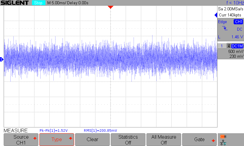
Rule of thumb: 99% of the (Gaussian distributed) noise peaks fall within 6x the rms value.
Points of attention when building this:
Although the circuit itself is quite simple, building it with care is essential for getting the right results. Note that here we are amplifying a high impedance microvolt source with a gain of 10.000 V/V. The picture of the breadboard prototype shows the correctly working circuit that was measured on. Attention should be given to:
1- Shielding E-fields:
The circuit should be in a fully closed metal box to prevent picking up electric field from the environment. An aluminium box is fine, magnetic shielding is not needed if you keep wires short.
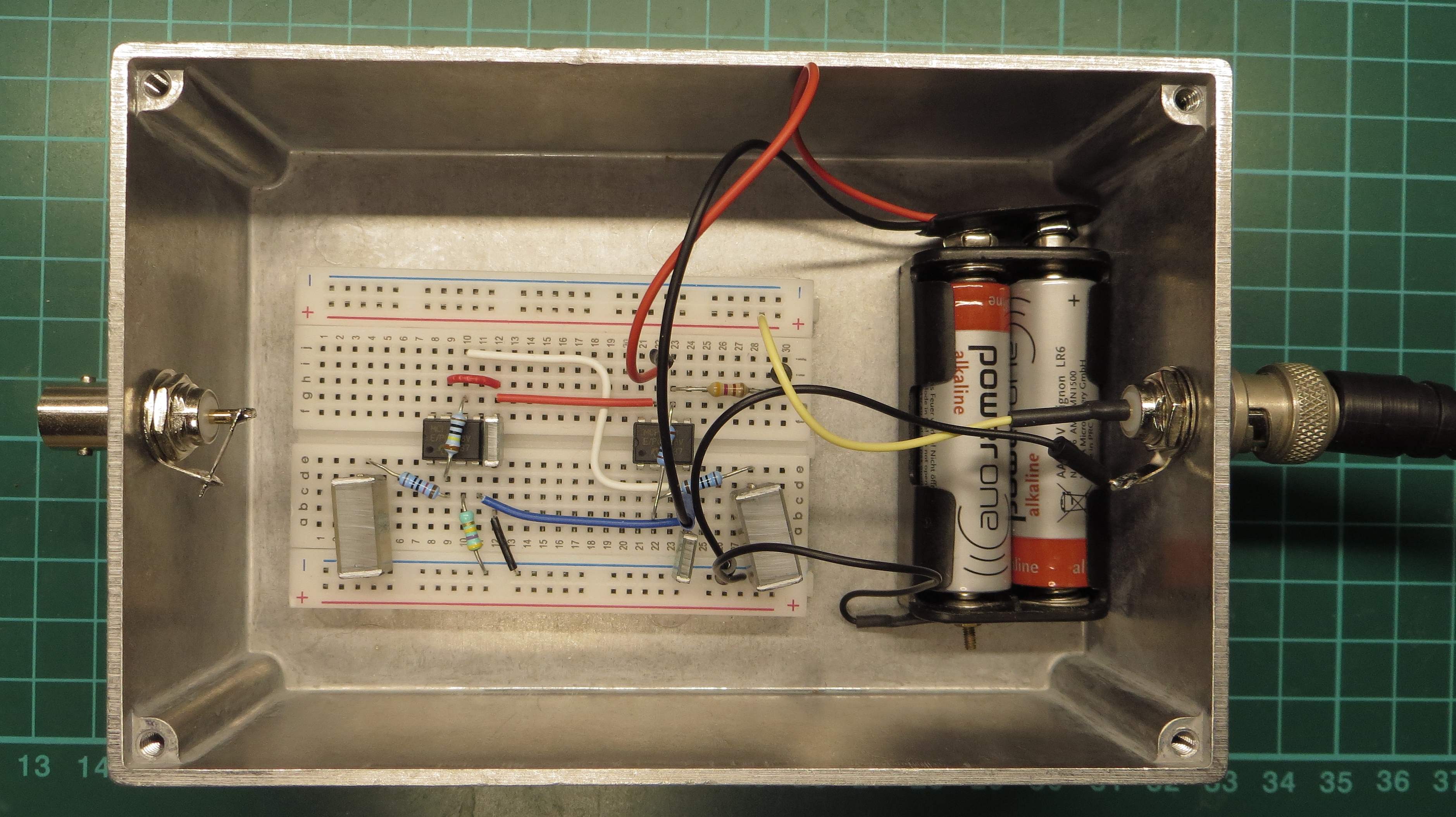
2-Prevent stray feedback from output to input for the circuit, this is the most important point: The first amplifier stage should be a few cm away from the second stage and also far away from the output wires to prevent capacitieve feedback to the noise resistor. For the same reason: use separate opamps, not a dual one. Keep the wires of the noise resistor as short as possible and mount it very close to the opamp input. Because total gain is +10201 V/V a stray feedback would result in gain (noise) peaking around 40kHz and in extreme cases even to oscillation. This is absent on the prototype shown but only after separating the amplifier stages, the first build version showed this peaking problem. To prevent this gain peaking you could change the second stage to an inverting amplifier (see circuit-inverted-option) but then you still would need a low stray feedback because otherwise it would restrict the bandwidth so I left it like this.
3-Microphonic pick-up:
tapping on the metal box with my breadboard prototype in it, I could hear a small amount of sound coming through the noise when connecting active speakers to the unit. Fix things and use some rubber feet underneath the box. Do use plastic film 2u2 capacitors and do not use ceramic X7R/Y5V/Z5U dielectric (most SMD) as these show piezoelectric behaviour and act as microphones making things worse.
4-Supply considerations:
A supply giving +1V5, 0V and -1V5 from a modified 2xAA battery holder was used.
Note the ground (0V) wire added to the node between the batteries in the holder (see picture prototype).
When using battery supply, adding 2x100nF supply decoupling at each opamp is enough.
Line power supply is likely not a good idea and switched mode supplies are a bad idea.
The circuit:
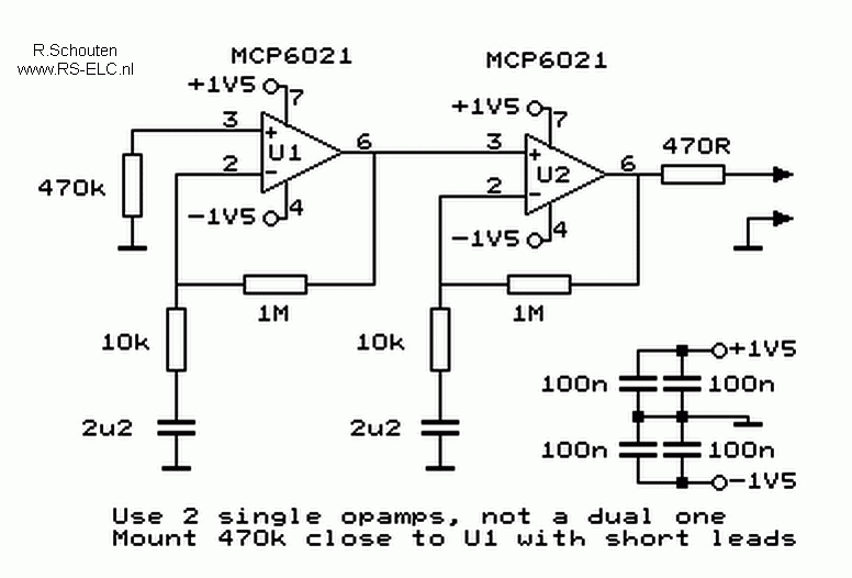
For the Pro's, some design considerations:
1-Selecting the value of the noise generating resistor Rn In general: Rn should have the highest possible value to maximise it's noise voltage.
Limitations determining the upper value of Rn:
Rn x Cin of the opamp forms a lowpass filter, we want 20kHz bandwidth within 1dB. Rn x Input current noise of the opamp (In) creates additional noise, this should be far below the Rn thermal noise. As this noise scales proportional with the value of Rn while it's thermal noise voltage only scales with the square root of Rn, this sets an upper value for Rn.
Opamp choice and some calculations:
For the MCP6021 opamp Cin is 6pF, we go for Rn=470k, that gives us -0.5dB at 20kHz (-3dB at 55kHz)
For the MCP6021 opamp In is 3fA/sqrtHz, that gives us a voltage noise of 3fAx470k= 1.4nV/sqrtHz
For the MCP6021 opamp Vn at 1kHz is 11nV/sqrtHz
The voltage noise of Rn should be at least 4x higher than the noise contributions of the opamp.
470k gives us 88nV/sqrtHz so all this is very acceptable.
Opamp details:
MCP6021 was chosen for reasons described below. Don't try opamps like TL071, they have too much voltage noise and current noise. -The opamp should have a CMOS input stage to provide low enough input current noise (below 20fA/sqrtHz is needed)
-The opamp should have a voltage noise below 15nV/sqrtHz at 1kHz and at below 60nV/sqrtHz at 20Hz.
-The opamp should have a gain-bandwidth product above 10MHz to have less than 1dB error for gain 100V/V at 20kHz
-The feedback resistors across the opamp stages should be maximum 3MOhm to prevent stray capacitance in the resistor package resulting in more than 0.5dB gain drop at 20kHz.(1Mohm was chosen here)
Circuit design hidden detail:
Opamps suffer from increasing noise at lower frequencies (called 1/F noise, happens below 100Hz) The MCP6021's 1/F noise would give around 1dB rise to the noise at the low end at 20Hz. This small increase was prevented by having capacitor values resulting in a low frequency -3dB cutt-off at 10Hz and some 1dB gain drop at 20Hz, that nicely compensates for this otherwise small increase.